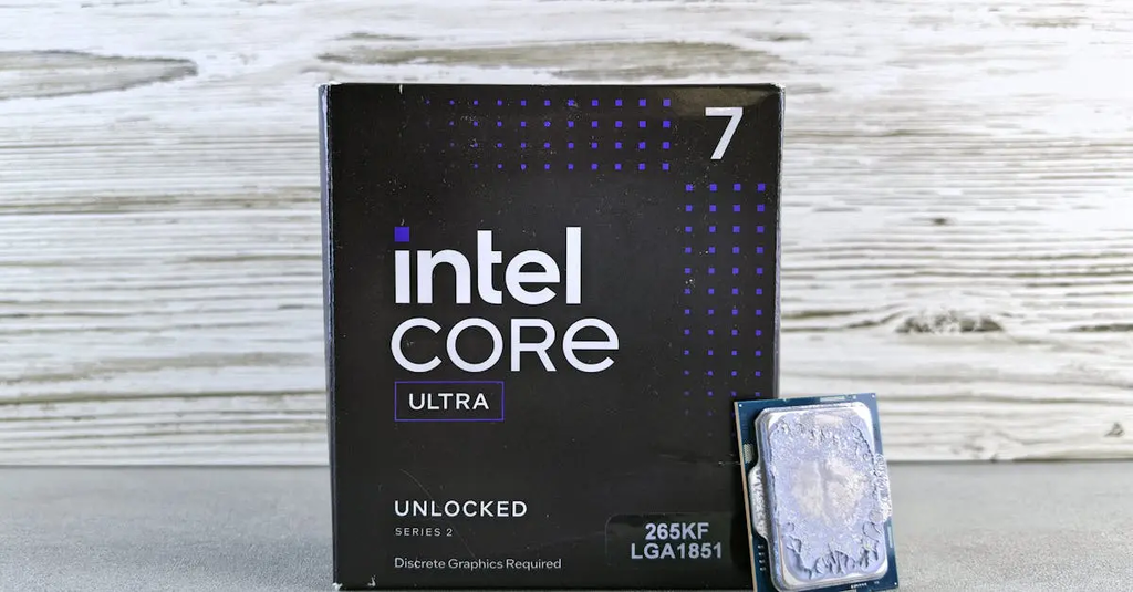
Component packaging and footprints
Component packaging and footprints in electronics refer to the physical casing and layout of electronic components. Packaging protects the internal circuitry and provides standardized shapes for handling and mounting. Footprints are the patterns of pads or holes on a printed circuit board (PCB) that match a component’s leads or terminals. Proper selection ensures compatibility between components and PCBs, influences assembly processes, and affects electrical performance, thermal management, and overall device reliability.
💡 Key Takeaways
- Distinguish common component packaging types (SMD, through-hole) and the footprints they require.
- Read a datasheet to identify the correct footprint—pad sizes, spacing, and land pattern tolerances.
- Design footprints with appropriate pad shapes, pad lengths, thermal/power pads, and solder mask clearances for reliable soldering.
- Account for manufacturing tolerances and assembly methods (reflow vs hand-solder) when selecting or creating footprints.
❓ Frequently Asked Questions
What is the difference between a component package and a footprint?
The package is the component's physical housing (shape, pins, thermal features) made by the manufacturer. The footprint is the PCB copper pattern that accepts the package, including pads, paste openings, and clearances.
Why is footprint accuracy important in PCB design?
Accurate footprints ensure reliable solder joints, proper mechanical fit, and correct electrical performance, reducing assembly defects like misalignment, shorts, or open connections.
What are common package types you’ll encounter on PCBs?
Common types include through-hole (e.g., DIP) and surface-mount (e.g., SOIC, QFP, QFN, BGA). Each type has distinct footprint conventions and soldering methods.
What are the key elements included in a footprint or land pattern?
Pads for pins, solder paste openings (for reflow), pad spacing (pitch), courtyard/keep-out areas, silkscreen marks, and a pin-1 indicator.
How can you verify a footprint matches a package?
Use the manufacturer's datasheet or official footprint, follow IPC-7351 guidelines, verify with a 3D model, and run DRC checks to confirm pin alignment and clearances.